1Overview
The Berkeley Nucleonics PVX-2506 is designed for pulsed I-V (current-voltage) characterization of semiconductor devices at up to 50 Volts and 10 Amps. It also suits other applications that call for high-current precision voltage pulses.
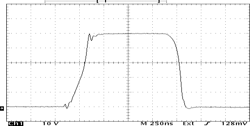
Pulsing the device and measuring during the pulse takes data before the device heats up. That approach circumvents the thermal effects of conventional DC testing, more closely approximates high-frequency operating characteristics, and avoids the activation of semiconductor "traps". A bi-directional MOSFET output stage built from fast power MOSFETs delivers fast rise and fall, minimal overshoot, undershoot, and ringing, and fast settling. The device under test stabilizes within a few hundred nanoseconds.
A quiescent (bias) voltage may be applied, holding the DUT at a non-zero voltage and then pulsing above or below it. The output pulse launches on a low-impedance cable that preserves pulse fidelity without distortion or ringing. The design is direct-coupled, air-cooled, and solid-state. Over-current detection and shut-down circuitry protects against arcs and shorts.
2How It Works
Conventional DC characterization holds a device at voltage and current long enough for it to heat. That self-heating shifts the measured curves and masks the behavior the device shows in real high-frequency operation. Pulsed I-V testing solves the problem by applying a short pulse and sampling the device during the pulse, before the junction temperature rises.
The benefit is threefold. Measuring inside a sub-microsecond pulse circumvents the thermal effects that distort DC data. It more closely approximates the high-frequency operating characteristics engineers actually care about. And it avoids the activation of semiconductor "traps", the charge-trapping mechanisms that slowly skew DC measurements.
The PVX-2506 requires three inputs. An external gate signal sets the timing, a pulse (VHIGH) DC supply input sets the pulse amplitude, and an optional quiescent (VLOW) DC supply input sets the bias level. Output pulse width and frequency follow the input gate. Output amplitude follows the VHIGH supply amplitude, with the optional VLOW supply setting a non-zero quiescent point that the output can pulse above or below.
The bi-directional output stage uses fast power MOSFETs to source and sink current, which is what gives the pulse its fast rise, fast fall, and clean settling. With minimal overshoot, undershoot, and ringing, the DUT reaches a stable operating point within a few hundred nanoseconds, leaving a wide measurement window inside even a short pulse.
3Specifications
All specifications are measured into a 5 Ohm load connected with a 4 foot output cable.
Input (VHIGH DC supply)
| Parameter | Specification |
|---|---|
| Maximum value | 75 Volts DC, floating |
| Minimum value | 0 Volts DC |
| Input connector | Screw terminals, rear panel |
Output
| Parameter | Specification |
|---|---|
| Maximum value | 50 Volts at 10 Amps |
| Minimum value | 0 Volts |
| Maximum current | 10 Amps |
| Means of adjustment | Controlled by pulse input |
| Pulse rise time | < 200 ns at 50 Volts (10% to 90%) |
| Typical settling time | < 400 ns including rise time |
| Pulse width | < 1 µs to 100 µs, controlled by gate input |
| Frequency range | Single-shot to 50 kHz, controlled by input gate |
| Maximum duty cycle | 0.50 (50%) |
| Output connector | 8-pin high-current D-sub |
Monitor Outputs
| Parameter | Specification |
|---|---|
| Voltage Monitor | 1 V/V into 1 MΩ, BNC front panel |
| Current Monitor | 0.1 A into 1 MΩ, BNC front panel |
Control Pulse Input
| Parameter | Specification |
|---|---|
| Source | External |
| Input level | +5 V ±1 V into 50 Ω |
| Rise time | < 20 ns |
| Gate input connector | BNC front panel |
General
| Parameter | Specification |
|---|---|
| Dimensions | 19 in rack mountable, 3 1/2 in x 17 in x 16 in |
| Support power | 100-240 VAC, 50/60 Hz |
4Monitoring & Front Panel
The PVX-2506 carries integral instrument-quality voltage and current probes that facilitate data acquisition. Both feed dedicated front-panel BNC monitor outputs, so the pulse can be observed and logged on a standard oscilloscope without external probes.
The Voltage Monitor delivers 1 V/V into a 1 MΩ load. Read the output pulse amplitude directly: one volt at the monitor corresponds to one volt at the DUT. The Current Monitor delivers 0.1 A into a 1 MΩ load, scaling the high-current pulse to a clean, low-level signal a scope can capture.
Pulsed and DC modes
Front-panel controls switch the instrument between pulsed mode and DC mode. In pulsed mode, the output follows the gate input to produce timed high-current pulses. In DC mode, the DC voltage from VHIGH is applied directly to the DUT, which is useful for setup, biasing checks, and steady-state reference measurements.
Connections
The gate signal enters on a front-panel BNC connector and sets pulse width and frequency. The high-current output leaves on an 8-pin high-current D-sub connector through a low-impedance cable that preserves pulse fidelity without distortion or ringing. The high-voltage VHIGH supply connects to rear-panel screw terminals rated to 75 Volts DC, floating, with the optional VLOW supply setting the quiescent bias point.
5Applications
- Pulsed I-V device characterization. Capture current-voltage curves at up to 50 V and 10 A before the device heats, for results that better reflect real operating conditions.
- Thermal-effect avoidance. Take data inside a sub-microsecond pulse to circumvent the self-heating that distorts conventional DC testing.
- Trap-state avoidance. Measure quickly enough to avoid activating semiconductor charge "traps" that skew slow DC sweeps.
- Quiescent-bias testing. Hold the DUT at a non-zero bias with the optional VLOW supply, then pulse above or below it to map behavior around an operating point.
- High-frequency behavior approximation. Approximate the high-frequency operating characteristics of power and RF semiconductor devices on a bench setup.
- High-current precision pulsing. Drive any application that needs clean, high-current voltage pulses with fast edges and low overshoot.
6Ordering Information
| Model | Description |
|---|---|
| PVX-2506 | 50 V, 10 A Precision Pulse Generator |
The low-impedance output cable that preserves pulse fidelity is included with the instrument. A pulse (VHIGH) DC supply input is required, and a quiescent (VLOW) DC supply input is optional, set above or below the pulse level to bias the device under test.
Contact
For a quote, configuration help, or application support, reach the Berkeley Nucleonics team.
Email: info@berkeleynucleonics.com
Phone: 800-234-7858