Product Data Sheet

Model 676 Arbitrary Waveform Generator

A high-performance, two-channel arbitrary waveform generator delivering 2.5 GS/s sampling, 14-bit vertical resolution, and 300 MHz bandwidth, with up to 64 Mpts of waveform memory per channel and rise and fall times under 1.1 ns. Optional 16 or 32-bit synchronized digital outputs make it a true mixed-signal source for the most demanding test environments.

Rider Series · Model 676 · Specifications preliminary, verify against published datasheet
Berkeley Nucleonics Model 676 arbitrary waveform generator

1Overview

The Berkeley Nucleonics Model 676 offers premium signal integrity through one of the easiest touch-screen interfaces in its class. The graphical user interface, Expert Rider, lets engineers build complex arbitrary waveforms and intricate modulations in a few clicks. Working in AWG mode, designers can add noise, apply filters, and import large sets of modulated data such as RF or I/Q waveforms.

The Model 676 is an affordable waveform generation platform that helps stretch a project's specifications to the limit, offering not just analog output but digital channels as well. In Amplified mode the analog output voltage adjusts up to 5 Vpp into a 50 ohm load. With analog bandwidth reaching 1 GHz on the DAC and AC paths, edges drop to 350 ps with minimal overshoot and ringing.

The instrument samples from 100 S/s up to 2.5 GS/s with 14-bit vertical resolution, delivering outstanding signal integrity. An optional 16 or 32-bit digital output adds up to 1.25 Gb/s of data per output in LVDS format. Combined and synchronized with the analog outputs, that mixed-signal capability makes the Model 676 an ideal generator for the most demanding technical applications.

2.5 GS/sSample Rate
14-bitVertical Resolution
300 MHzBandwidth
64 MptsMemory / Channel
< 1.1 nsRise / Fall
Model 676 front panel with touch display and analog and digital output connectors
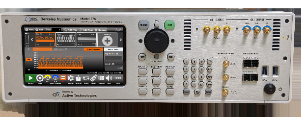
Model 676 front panel: 7-inch capacitive touch display, dual analog channels, marker outputs, and Mini-SAS HD digital output ports.

2Key Features

Two Analog Channels

Dual independent analog outputs, configurable as single-ended, differential, or AC coupled.

2.5 GS/s, 14-bit

Best-in-class DAC technology at an affordable price for ultra-wideband signal generation.

300 MHz Bandwidth

Wideband output with fast edges and clean transitions across the operating range.

Up to 64 Mpts Memory

Deep waveform memory per channel, scalable from a standard 1 Mpts up to 64 Mpts.

Edges Under 1.1 ns

Rise and fall times below 1.1 ns track the parameters of fast power devices.

Mixed-Signal Output

Optional 16 or 32-bit LVDS digital outputs, synchronized with the analog channels.

Touch Interface

7-inch capacitive touch display with swipe gestures and a virtual numeric keypad.

Multi-Unit Sync

Synchronize up to four instruments into a single 8-channel waveform generation system.

The Model 676 gives users access to the best-in-class DAC technology at an affordable price. The 2.5 GS/s sample rate and 14-bit vertical resolution help generate ultra-wideband communication signals with 1 GHz modulation bandwidth, 2 GHz in I/Q modulation, and less than -60 dBc SFDR across each channel. The analog channels can be configured as differential, single-ended, or AC coupled, eliminating the need for baluns or hybrids in the test path.

3User Interface

The Model 676 interface is designed for touch and developed to put the capabilities of a modern waveform generator at your fingertips. All instrument controls and parameters are reached through an intuitive UI that recalls the simplicity of a tablet or smartphone. Touch features and gestures let engineers and scientists create advanced waveforms or digital patterns in a few touches.

  • The swipe gesture gives easy access to the output waveform parameters.
  • A touch-friendly virtual numeric keypad improves the experience of entering data.
  • Time-saving shortcuts and intuitive icons simplify instrument setup.
Simple Rider AFG mode screen showing carrier setup, waveform preview, and channel status
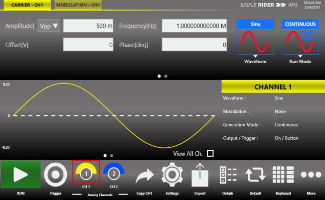
Simple Rider, AFG mode: carrier setup, live waveform preview, run-mode selection, and per-channel status in a touch-first layout.

4Mixed-Signal Generation & Multi-Unit Sync

The Model 676 carries optional 16 or 32-bit digital outputs, synchronized with the corresponding analog channels in two 16-bit groups. Each group can be configured as 8-bit full speed, with bit rate at half the sampling rate, or 16-bit low speed, with bit rate at one quarter of the sampling rate. Mixed-signal generation is a strong solution for digital design and validation, system synchronization, and DAC and ADC testing.

The digital output pins meet native LVDS standards. A digital cable to SMA adapter is available, and for slower applications, LVDS to LVTTL converters are offered as well.

In Advanced mode, users can define complex waveforms with up to 16,384 entries of analog waveforms and digital patterns in a sequence, in terms of loops, jumps, and conditional branches. In Multi-sequence mode, two sequences can control Channel 1 and Channel 2, and the corresponding digital channels, separately as generators. Up to four instruments can be synchronized together to build a real 8-channel waveform generation system, which is extremely useful in applications such as MIMO where many channels are needed.

Expert Rider sequencer showing analog and digital waveform entries in a multi-step sequence
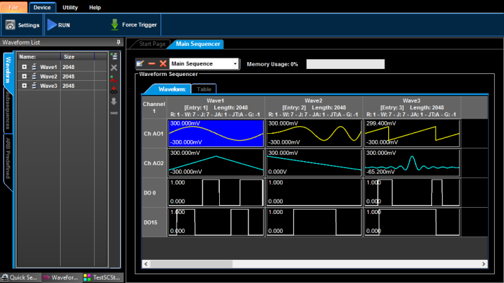
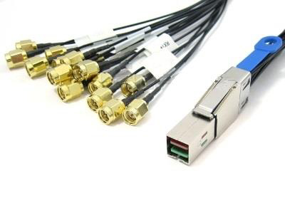
Expert Rider sequencer: per-entry analog (Ch AO1 / Ch AO2) and digital (DO 0 / DO 15) waveforms across a multi-step sequence.
Mini-SAS HD to SMA breakout cable for digital outputs
Proprietary Mini-SAS HD to SMA cable breaks the LVDS digital outputs out to 16 SMA connectors for bench use.

5Specifications: Channels & Operating Modes

ParameterSpecification
Number of Channels
Analog2
Digital out16 or 32-bit (optional)
Marker out2
Operating Mode
AFG modeBasic Operation Mode (DDS mode)
True Arb modeStandard waveforms: Sine, Square, Pulse, Ramp, and more (Noise, DC, Sin(x)/x, Gaussian, Lorentz, Exponential Rise, Exponential Decay, Haversine)
AFG run modesContinuous, modulation, sweep, burst
Basic Operation (DDS) Mode
Sampling clock2.5 GS/s, fixed
Vertical resolution14-bit
Arbitrary waveform length16,384 points
Advanced Operation Mode
Run modesContinuous, sequencer, triggered, gated
Vertical resolution14-bit
Waveform length64 to 64 M points (1 M = 220) in multiples of 64 points for length < 320 points, multiples of 16 points for length ≥ 320 points
Memory optionsStandard 1 M points; optional 16 M, 32 M, 64 M points

6Specifications: Basic Mode Output

ParameterSpecification
ConnectorsSMAs for DC AMP on front panel
Output typeSingle-ended or differential
Output impedance50 ohm (single-ended) or 100 ohm (differential)
Frequency Range
Sine1 uHz to 600 MHz
Square, Pulse1 uHz to 330 MHz
Ramp, Exponential Rise, Exponential Decay1 uHz to 30 MHz
Sin(x)/x, Gaussian, Lorentz, Haversine1 uHz to 60 MHz
Arbitrary1 uHz to 400 MHz
Frequency Resolution & Accuracy
Resolution (Sine, Square, Pulse, Arbitrary, Amp, Sin(x)/x, Gaussian, Lorentz)1 uHz or 15 digits
Resolution (Exponential Rise, Exponential Decay, Haversine)1 uHz or 14 digits
Accuracy (non-ARB)±10e-6 of setting
Accuracy (ARB)±10e-6 of setting ±1 uHz
Sine flatness (1 Vp-p, relative to 1 kHz, typical)DC to 600 MHz: ±0.5 dB

7Specifications: Sine, Square & Pulse

Sine Waves

ParameterSpecification
Harmonic distortion (1 Vp-p)1 uHz to ≤ 10 MHz: < -60 dBc; > 10 MHz to ≤ 50 MHz: < -55 dBc; > 50 MHz to ≤ 200 MHz: < -40 dBc; > 200 MHz to ≤ 600 MHz: < -28 dBc
Total harmonic distortion (1 Vp-p, typical)10 Hz to 20 kHz: < 0.1%
Spurious (1 Vp-p)1 uHz to ≤ 10 MHz: < -65 dBc; > 10 MHz to ≤ 330 MHz: < -55 dBc; > 330 MHz to ≤ 500 MHz: < -50 dBc; > 500 MHz to ≤ 600 MHz: < -40 dBc
Phase noise (1 Vp-p, 10 kHz offset, typical)1 MHz: < -115 dBc/Hz; 10 MHz: < -110 dBc/Hz; 100 MHz: < -105 dBc/Hz; 600 MHz: < -90 dBc/Hz

Square Waves

ParameterSpecification
Rise / fall time (typical)1 ns
Overshoot (1 Vp-p, typical)< 2%
Jitter (rms, typical)< 10 ps

Pulse Waves

ParameterSpecification
Pulse width1 ns to (Period - 1 ns)
Resolution10 ps or 15 digits
Pulse duty0.1% to 99.9% (pulse width limitations apply)
Leading / trailing edge transition time800 ps to 1000 s
Edge resolution1 ps or 15 digits
Overshoot (1 Vp-p, typical)< 2%
Jitter (rms, typical)< 10 ps with leading / trailing edge transition time ≥ 1 ns

Ramp & Other Waves

ParameterSpecification
Ramp linearity (< 10 kHz, 1 Vp-p, 100% symmetry, typical)≤ 0.1%
Ramp symmetry0% to 100%
Noise bandwidth (-3 dB, typical)400 MHz
Noise addWhen activated, output signal amplitude is reduced to 50%
Noise level0.0% to 50% of amplitude (Vp-p) setting, resolution 0.1%

Arbitrary

ParameterSpecification
Number of samples2 to 16,384
Analog bandwidth (-3 dB, typical)400 MHz
Rise / fall time (typical)< 800 ps
Jitter (rms, typical)400 ps

8Specifications: Amplitude, Offset & DC

DC

ParameterSpecification
Range (50 ohm, single-ended)-2.5 V to 2.5 V
Accuracy±(1% of |setting| + 5 mV)

Amplitude

ParameterSpecification
Range (50 ohm, single-ended)1 uHz ~ 350 MHz: 5 mVp-p to 5 Vp-p; 350 MHz ~ 550 MHz: 5 mVp-p to 3 Vp-p; 550 MHz ~ 600 MHz: 5 mVp-p to 2 Vp-p
Range (100 ohm, differential)1 uHz ~ 350 MHz: 10 mVp-p to 10 Vp-p; 350 MHz ~ 550 MHz: 10 mVp-p to 6 Vp-p; 550 MHz ~ 600 MHz: 10 mVp-p to 4 Vp-p
Accuracy (1 kHz sine, 0 V offset, > 5 mVp-p, 50 ohm load)±(1% of setting + 5 mV)
Resolution1 mVp-p or 4 digits
Output impedanceSingle-ended: 50 ohm; Differential: 100 ohm

Vocm

ParameterSpecification
Range (50 ohm load, single-ended)-2.5 V to +2.5 V
Range (High Z load, single-ended)-5 V to +5 V
Accuracy (50 ohm load, single-ended)±(1% of |setting| ±5 mV)
Resolution1 mV or 4 digits

Offset

ParameterSpecification
Range (50 ohm load, single-ended)±(2.5 Vpk - Amplitude ÷ 2)
Range (High Z load, single-ended)±(5 Vpk - Amplitude ÷ 2)
Accuracy (50 ohm load, single-ended)±(1% of |setting| + 5 mV)
Resolution1 mV or 4 digits

Window

ParameterSpecification
Range (50 ohm load, single-ended)1 uHz ~ 350 MHz: -5 V to +5 V; 350 MHz ~ 550 MHz: -4 V to +4 V; 550 MHz ~ 600 MHz: -3.5 V to +3.5 V
Range (100 ohm, differential)1 uHz ~ 350 MHz: -10 V to +10 V; 350 MHz ~ 550 MHz: -8 V to +8 V; 550 MHz ~ 600 MHz: -7 V to +7 V
Range (High Z, single-ended)1 uHz ~ 350 MHz: -10 V to +10 V; 350 MHz ~ 550 MHz: -8 V to +8 V; 550 MHz ~ 600 MHz: -7 V to +7 V

9Specifications: Modulation

Amplitude Modulation (AM)

ParameterSpecification
Carrier waveformsInternal or external
Modulation sourceInternal or external
Internal modulating waveformsSine, Square, Ramp, Noise, ARB
Modulating frequencyInternal: 500 uHz to 50 MHz; External: 10 MHz maximum
Depth0.00% to 120.00%

Frequency Modulation (FM)

ParameterSpecification
Carrier waveformsStandard waveforms (except Pulse, DC and Noise), ARB
Modulation sourceInternal or external
Internal modulating waveformsSine, Square, Ramp, Noise, ARB
Modulating frequencyInternal: 500 uHz to 50 MHz; External: 10 MHz maximum
Peak deviationDC to 300 MHz

Phase Modulation (PM)

ParameterSpecification
Carrier waveformsStandard waveforms (except Pulse, DC and Noise), ARB
Modulation sourceInternal or external
Internal modulating waveformsSine, Square, Ramp, Noise, ARB
Modulating frequencyInternal: 500 uHz to 50 MHz; External: 10 MHz maximum
Phase deviation range0° to 360°

Frequency Shift Keying (FSK)

ParameterSpecification
Carrier waveformsStandard waveforms (except Pulse, DC and Noise), ARB
Modulation sourceInternal or external
Internal modulating waveformsSquare
Key rateInternal: 500 uHz to 50 MHz; External: 10 MHz maximum
Hop frequency1 uHz to 600 MHz
Number of keys2

Phase Shift Keying (PSK)

ParameterSpecification
Carrier waveformsStandard waveforms (except Pulse, DC and Noise), ARB
Modulation sourceInternal or external
Internal modulating waveformsSquare
Key rateInternal: 500 uHz to 50 MHz; External: 10 MHz maximum
Hop phase0° to +360°
Number of keys2

Pulse Width Modulation (PWM)

ParameterSpecification
Carrier waveformsPulse
Modulation sourceInternal or external
Internal modulating waveformsSine, Square, Ramp, Noise, ARB
Modulating frequencyInternal: 500 uHz to 50 MHz; External: 10 MHz maximum
Deviation range0% to 50% of pulse period

10Specifications: Sweep & Burst

Sweep

ParameterSpecification
TypeLinear, logarithmic, staircase, and user defined
WaveformsStandard waveforms (except Pulse, DC and Noise), ARB
Sweep time50 us to 2000 s
Hold / return times0 to (2000 s - 50 us)
Sweep / hold / return time resolution20 ns or 12 digits
Total sweep time accuracy (typical)≤ 0.4%
Start / stop frequency rangeSine: 1 uHz to 600 MHz; Square: 1 uHz to 300 MHz
Trigger sourceInternal / external / manual

Burst

ParameterSpecification
WaveformsStandard waveforms (except DC and Noise), ARB
TypeTrigger or gated
Burst count1 to 1,000,000 cycles or infinite
Internal trigger delay0 to 100 s
Internal trigger delay accuracy (typical)±(0.1% setting + 5 ps)
Internal trigger rate0 to 500 s
Internal trigger interval range1 us to 500 s
Internal trigger resolution2 ns or 12 digits

11Specifications: Advanced Mode Output

ParameterSpecification
ConnectorsSMAs for AMP, DAC, and AC modes on front panel
Output typeAMP and DAC modes: single-ended or differential; AC mode: single-ended
Output impedance50 ohm single-ended, 100 ohm differential
Channel Skew
Skew control (between channels) range0 to 240,000 ps
Skew control resolution10 ps
Skew control accuracy±(10% of setting + 20 ps)
Skew between positive and negative outputs (typical)≤ 20 ps
Initial skew< 200 ps from 1.25 GS/s to 2.5 GS/s; < 1 ns below 1.25 GS/s
Marker Skew
Range0 to 101,790 ps
Resolution78 ps
Accuracy (typical)±(10% of setting + 140 ps)
Initial skew< 1.4 ns from 1.25 GS/s to 2.5 GS/s; < 2 ns from 100 MS/s to 1.25 GS/s; < 4.5 ns below 100 MS/s
Calculated Bandwidth (0.35 / rise or fall time, typical)
AMP460 MHz
DAC1 GHz
AC1 GHz
Amplitude Range (single-ended, 50 ohm load)
AMP0 to 5 Vp-p (doubled for differential or High Z load)
DAC0 to 0.8 Vp-p (doubled for differential or High Z load)
AC0 to 2 Vp-p (doubled for High Z load)
Amplitude, Offset & Vocm
Amplitude accuracy (AMP, DAC; 1 kHz sine, 0 V offset)±(1% of setting + 5 mVp-p)
Amplitude accuracy (AC; 100 MHz sine, 0 V offset, typical)±(2% of setting + 5 mVp-p) - 0.1% of |setting| x temperature deviation
Amplitude resolution (AMP, DAC, AC)0.1 mV or 5 digits
Offset range (AMP, single-ended 50 ohm)-2.5 V to +2.5 V (doubled for differential or High Z load)
Offset range (DAC, single-ended 50 ohm)-0.35 V to +0.35 V (doubled for differential or High Z load)
Offset accuracy (AMP, DAC)±(1% of |setting| + 5 mV)
Offset resolution (AMP, DAC)10 mV or 3 digits
Vocm range (AMP, single-ended 50 ohm)-2.5 V to +2.5 V (doubled for differential or High Z load)
Vocm range (DAC, single-ended 50 ohm)-0.35 V to +0.35 V (doubled for differential or High Z load)
Vocm accuracy (AMP)±(1% of setting + 5 mV)
Vocm accuracy (DAC)±(6% of Vocm range + 5 mV)
Vocm resolution (AMP, DAC)10 mV or 3 digits
Voltage Window Range (single-ended, 50 ohm load)
AMP1 uHz to 300 MHz: -5 V to 5 V; > 300 MHz to 550 MHz: -4 V to 4 V; > 550 MHz to 600 MHz: -3.5 V to 3.5 V (doubled for differential or High Z load)
DAC-0.4 V to 0.4 V (doubled for differential or High Z load)
AC-1 V to 1 V (doubled for High Z load)
Harmonic Distortion (Sine 32 points at 2.5 GS/s, 78.125 MHz, typical)
AMP (1 Vp-p single-ended)< -56 dBc (single-ended or differential)
DAC (0.5 Vp-p single-ended)< -60 dBc (single-ended or differential)
AC (1 Vp-p single-ended)< -56 dBc
Spurious (Sine 32 points at 2.5 GS/s, 78.125 MHz, typical)
AMP (1 Vp-p single-ended)< -62 dBc (single-ended or differential)
DAC (0.5 Vp-p single-ended)< -62 dBc (single-ended or differential)
AC (1 Vp-p single-ended)< -55 dBc
SFDR (Sine 32 points at 2.5 GS/s, 78.125 MHz, typical)
AMP (1 Vp-p single-ended)< -56 dBc (single-ended or differential)
DAC (0.5 Vp-p single-ended)< -60 dBc (single-ended or differential)
AC (1 Vp-p single-ended)< -55 dBc
Rise / Fall Time (10% to 90%, typical)
AMP (1 Vp-p single-ended)< 800 ps
DAC (0.5 Vp-p single-ended)< 350 ps
AC (1 Vp-p single-ended)< 350 ps
Overshoot (typical)
AMP (1 Vp-p single-ended)< 2% at 800 ps
DAC (0.5 Vp-p single-ended)< 1% at 450 ps
AC (1 Vp-p single-ended)< 2% at 450 ps
Timing & Clock
Random jitter on clock pattern (AMP, DAC; rms, typical)< 5 ps
Total jitter on random pattern (AMP, DAC; peak-to-peak at 625 Mb/s, PRBS 15, typical)< 150 ps

12Specifications: Digital Outputs (Optional)

ParameterSpecification
ConnectorsMini-SAS HD connector on front panel
Number of connectors2
Number of outputs32-bit (16-bit x 2 groups)
Output impedance100 ohm differential
Output typeLVDS
Rise / fall time (10% to 90%, typical)600 ps
Initial skew between digital outputs (typical)< 500 ps between group A and B
Jitter (peak-to-peak, 2.5 GS/s, 1.25 Gb/s, PN15 pattern, BER = 1e-12)150 ps
Maximum update rate1.25 Gbps (full-speed mode, max 16-bit); 625 Mbps (low-speed mode, max 32-bit)
Memory depth (optional)Half of analog waveform length (full-speed mode), one fourth of analog waveform length (low-speed mode)

8-bit LVDS to LVTTL Converter Probe (Optional AT-DLL8)

ParameterSpecification
Output connector20-position 2.54 mm 2-row IDC header
Output typeLVTTL
Output impedance50 ohm nominal
Output voltage0.8 V to 3.8 V, programmable in groups of 16 bits
Maximum update rate125 Mbps at 0.8 V, 400 Mbps at 3.6 V
Dimensions2 in x 0.9 in x 3 in (52 mm x 22 mm x 76 mm)
Cable1 meter, proprietary standard

Mini-SAS HD to SMA Cable (Optional)

ParameterSpecification
Output connectorSMA
Output typeLVDS
Number of SMA16 (8 bits)
Cable1 meter, proprietary standard

13Specifications: Auxiliary I/O & Clock

Marker Out

ParameterSpecification
Connector typeSMA on front panel
Number of connectors2 (1 for each analog output)
Output impedance50 ohm
Output level (into 50 ohm)1 V to 2.5 V, resolution 10 mV, accuracy ±(2% setting + 10 mV) typical
Variable delay control0 to 60,606 ps, resolution 78 ps, accuracy ±(10% of setting + 140 ps) typical
Rise / fall time (10% to 90%, 2.5 V, typical)800 ps
Total jitter (random pattern, 2.5 GS/s, 1.25 Gb/s, PN15, 2.5 V, BER = 1e-12)155 ps

Trigger / Gate Input

ParameterSpecification
ConnectorSMA on front panel
Input impedance1.1 kohm
Slope / polarityPositive or negative selectable
Input damage level< -15 V or > +15 V
Threshold control level-10 V to 10 V, resolution 50 mV, accuracy ±(10% of |setting| + 0.2 V) typical
Input voltage swing0.5 Vp-p minimum
Minimum pulse width12 ns
Initial trigger / gate delay to analog outputBasic mode: 384.6 ns ±50 ps; Advanced mode: 20 ns + 2288 sampling clock cycles ±1 sampling clock cycle
Trigger in to output jitter (typical)< 50 ps

Sync, Reference & External Clock

ParameterSpecification
Sync In / OutInfiniband 4X connector on rear panel; master to slave delay 48.6 ns typical
Reference clock inputSMA on rear panel, 50 ohm AC coupled; -5 dBm to 4 dBm sine or square; damage +8 dBm or ±15 VDC max; 10 MHz to 80 MHz variable
Reference clock outputSMA on rear panel, 50 ohm AC coupled; 10 MHz; accuracy ±1.0 x 10e-6; aging ±1.0 x 10e-6/year; 1.6 Vp-p into 50 ohm, 3.2 Vp-p into Hi-Z; jitter 11.5 ps rms typical
External sampling clock inputSMA on rear panel, 50 ohm AC coupled; 2 inputs (1 per channel); 1.25 GHz to 2.5 GHz; -5 dBm to 4 dBm; damage +8 dBm or ±15 VDC max
External modulation inputSMA on rear panel, 10 kohm; 2 inputs (1 per channel); 10 MHz bandwidth with 50 MS/s sampling; -1 V to +1 V (except FSK, PSK); FSK, PSK: 3.3 V; 14-bit vertical resolution

14Specifications: Power & Environmental

Power

ParameterSpecification
Voltage range100-240 VAC ±10%
Frequency range47-63 Hz
Max power consumption120 W

Environmental

ParameterSpecification
Temperature (operating)32 F to 122 F (0 C to +50 C)
Temperature (non-operating)-4 F to 185 F (-20 C to +85 C)
Humidity (operating)8% to 90% RH, max wet-bulb 29 C at or below +50 C (derates to 20.6% RH at +50 C). Non-condensing.
Humidity (non-operating)5% to 98% RH, max wet-bulb 40 C at or below +60 C (derates to 29.8% RH at +60 C). Non-condensing.
Altitude (operating)10,000 ft (3,048 m)
Altitude (non-operating)39,370 ft (12,000 m)

EMC & Safety

ParameterSpecification
SafetyUL61010-1, CAN/CSA C22.2 No.61010-1, EN61010-1, IEC61010-1
EmissionsCISPR 11 Class A, EN61000-3-2:2006, EN 61000-3-3:1995
ImmunityEN 61326-1:2006, IEC 61000-4-2:2001, -4-3:2002, -4-4:2004, -4-5:2001, -4-6:2003, -4-11:2004
Regional certificationsEuropean Union: EN61326-1; Australia / New Zealand: CISPR 11:2003

15Specifications: System & Connectors

ParameterSpecification
Display7-inch, 1024 x 600, capacitive touch LCD
Operating systemWindows 10
External dimensions17.5 in x 5.3 in x 12.5 in (445 mm x 135 mm x 320 mm), 3U 19-inch rackmount
Weight21.4 lb (9.7 kg)
Hard disk256 GB SSD
ProcessorIntel i3-4170, 3.7 GHz or better
Processor memory8 GB
Front panel connectorsCH1 OUTPUT +/- (SMA), CH1 AC (SMA), CH2 OUTPUT +/- (SMA), CH2 AC (SMA), MARKER OUT 1 and 2 (SMA), TRG.IN (SMA), DIGITAL POD A/B/C/D [7..0], 2 USB 3.0 ports
Rear panel connectors
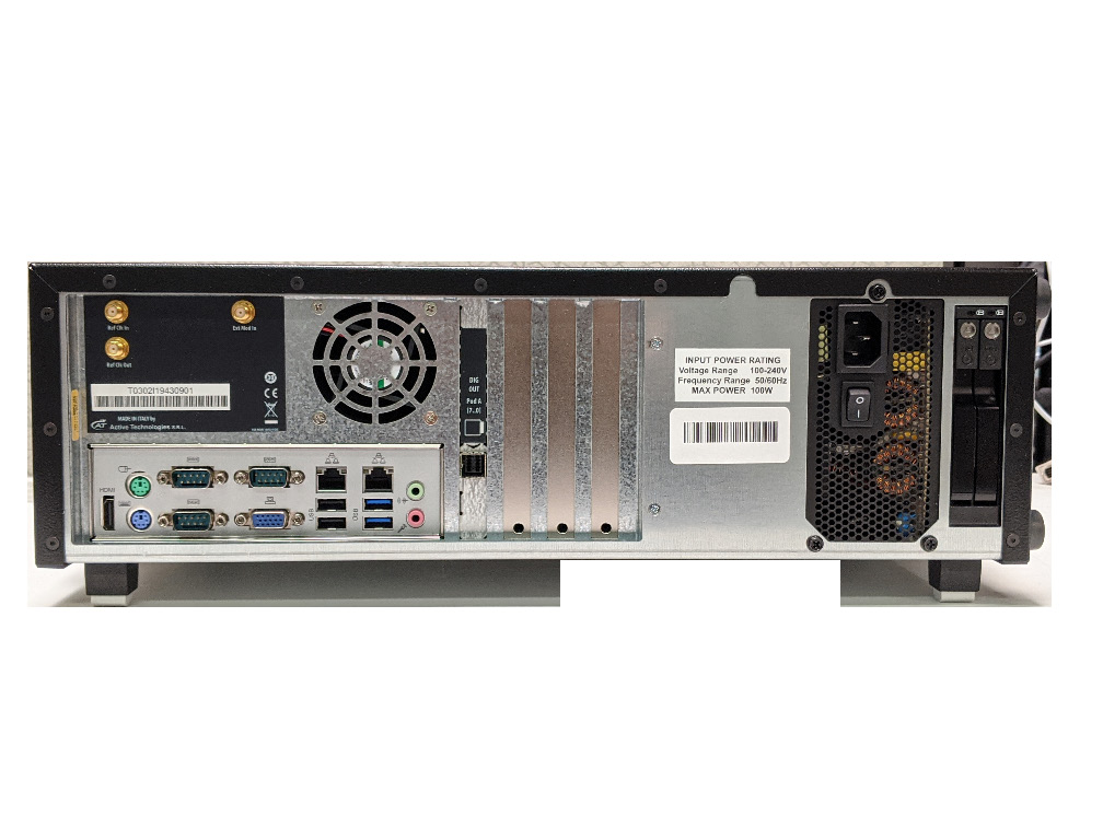
Ref. Clk. IN (SMA), Ext. Clk. In Ch1/Ch2 (SMA), Ext. Mod. In Ch1/Ch2 (SMA), Ref. Clk. Out (SMA), Sync. Out/In (Infiniband 4X), Pattern Jump In (DSUB-15), External monitor (DVI, VGA), 4 USB 2.0 ports, 2 USB 3.0 ports, Ethernet (10/100/1000BaseT, RJ45), Audio In/Out, 2 PS/2 ports
Model 676 rear panel showing clock, sync, USB, Ethernet, monitor, and AC power connectors
Model 676 rear panel: reference and external clock SMAs, Sync In/Out, monitor ports, USB, Ethernet, and the AC power inlet.

16Applications

The Model 676 serves a broad range of demanding test environments where signal integrity, fast edges, and a wide dynamic range matter.

Semiconductor Testing

Semiconductor engineers find the ability to emulate noisy or distorted waveforms useful for testing component compliance. The fast edges and pulse generation of the Model 676 track the parameters of fast power devices.

  • Clock and sensor signal generation
  • MOSFET gate-drive amplitude signal emulation
  • Power-up sequences of ICs using the low-impedance feature (5 ohm output impedance)
Close view of a populated circuit board with processors and power components
Fast edges and pulse generation make the Model 676 well suited to characterizing fast power devices and semiconductor components.

Automotive

Today's vehicles rely on sophisticated electronic control units with sensitive components. Combining 2.5 GS/s with 14-bit vertical resolution, the Model 676 is an ideal tool for the new testing challenges in automotive.

  • CAN, CAN-FD, LIN, FlexRay, and SENT emulation
  • EMI debugging, troubleshooting, and testing
  • Electrical standards emulation up to 20 V
  • Power MOSFET circuitry optimization in automotive electronics

IoT and Industry 4.0

The Model 676 can emulate complex RF I/Q modulation and test against wireless devices for Internet of Things and Industry 4.0 applications. Engineers can import waveforms to emulate devices under test, imposing distortions such as noise to verify whether devices comply with standards.

Research

Research centers and universities are key users of the Model 676, which produces complex waveforms, multilevel signals, and pulse emulation based on variable edges. The combination of fast edge generation, excellent dynamic range, and a simple user interface meets the demands of intensive experiments such as accelerators, tokamaks, and synchrotrons, all while saving on the cost of custom test boards.

  • Emulation of detectors
  • Emulation of signal sources with added noise
  • Generation and playback of real-world signals
  • Emulation of long PRBS sequences
  • Modulating and driving laser diodes

Aerospace and Defense

The Model 676 works well with electronic warfare signals, such as those produced by radar or sonar systems. It can be fitted into a modular system for radio or I/Q signal modulation, and it creates pulses useful in pulsed electron beams, x-ray sources, flash x-ray radiography, lightning pulse simulators, and high-power microwave modulators.

  • Frequency response, intermodulation distortion, and noise-figure measurements
  • Phase-locked loop (PLL) pull-in and hold-range characterization
  • Radar base-band signal emulation
Large radio telescope dishes against a night sky
Radio and I/Q signal modulation for research, communications, and defense systems.
Mobile military radar system deployed in the field
Electronic warfare and radar base-band signal emulation for aerospace and defense.

17Software & Support

The Model 676 runs the Rider software environment. Simple Rider drives the AFG and basic generation modes through a clean, touch-first layout for quick setup. Expert Rider opens the full Advanced mode, where users build sequences with loops, jumps, and conditional branches, add noise and filters, and import large modulated data sets such as RF or I/Q waveforms.

Both environments are available for download:

Request the full datasheet. This document summarizes the Model 676. For the complete published datasheet, ordering options, and configuration support, contact Berkeley Nucleonics.

Contact

For a quote, configuration help, or application support, reach the Berkeley Nucleonics team.

Email: info@berkeleynucleonics.com
Phone: 800-234-7858

Berkeley Nucleonics Corporation, 2955 Kerner Blvd, San Rafael, CA 94901.