1. Safety
The high-power nature of this device dictates the use of caution when operating or servicing this equipment. Observe all safety precautions listed below. Failure to do so could result in injury or death.
Precautions
- The Laser Diode Driver should be serviced only by personnel experienced in high-power pulsed-power systems.
- Service personnel should be instructed to observe all safety precautions as stated in the operating instructions, and those safety precautions standard to the high-voltage pulsed-power community. Failure to do so could result in serious injury.
- Do not handle the load or terminations, or remove the input or output cables, while the driver is in operation. Ensure that the 24 VDC power supply has fully discharged before handling the load. Failure to observe these precautions can result in potential electric shock to personnel, arcing, and damage to the connectors and system.
- The Laser Diode Driver contains reference planes which are elevated to the potential of the output pulse. Extreme caution should be exercised when servicing the equipment.
- The Laser Diode Driver contains electrolytic capacitors. Do not reverse the polarity of the input DC power supply, and do not exceed the maximum ratings for the support power supplies. Doing so may result in damage to the capacitors or to the driver, or personal injury due to venting of the capacitors.
- Pulsed-power systems are capable of random triggering via transients. Therefore, when the driver is turned on, or high voltage is present in the module, assume it is possible to get a pulse on the output stripline.
Berkeley Nucleonics Corporation (BNC) provides information on its products and associated hazards, but it assumes no responsibility for the after-sale operation and safety practices.
2. Overview
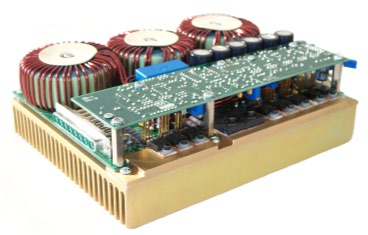
The PCO-6131 is a compact, OEM-style high-power pulsed current source designed to drive diode lasers, bars, and arrays in pulsed, QCW, or CW modes. It delivers output current variable from 1 A to 125 A, pulse widths variable from <100 ns to DC, and pulse repetition frequencies variable from single-shot to 500 kHz at duty cycles up to 100%.
The PCO-6131 is based on a hysteretic, average-current, switch-mode regulator. This type of regulator is a variable-frequency, variable-pulse-width design which maintains current in an energy-storage inductor between a minimum and maximum level. The ripple is limited to the minimum and maximum current determined by the hysteretic controller. The controller turns on to charge the energy-storage inductor when the current drops to the lower limit and turns off when the current reaches the upper limit, and repeats this operation as necessary to maintain the proper current. The time for these operations varies depending on the load voltage and the input voltage. Therefore the pulse width of the controller will change as necessary to charge the inductor, and the period will change depending on the rate at which the inductor discharges. The relationship for this operation is represented by V = L di/dt.
When the output is shorted, such as when no pulse is being output, the voltage applied to the inductor is 24 volts. This results in a very fast increase in current, so very short on-times are necessary. When the controller switches off, a very small voltage is across the inductor, so the current decays very slowly and therefore the off-time is quite large. All this reverses when the output is connected to a load. When the load is near the maximum V, the time to charge the inductor is very large but the decay time is very short. The advantage of this controller is that the current is controlled to an upper and lower limit regardless of the pulse width. It can generate short or long pulses and performs as a current source.
The current regulator is started when the TTL "enable" line is taken high and runs as long as the enable is high. This happens when the control gate is taken high and continues until the gate control is taken low. It takes a finite time for the current source to charge to the proper current (a ramp-up time), after which a pulse can be generated. The use of the hysteretic regulator provides a large input range and high efficiency.
The current source is combined with a crowbar (shorting switch). The shunting crowbar switch shorts the output of the regulator until output current is needed. The pulse is generated by opening the shunt switch for the length of the input pulse. A pulse is generated when the control gate is high: the shunt switch is opened for the length of the input control gate, forcing the current to flow through the laser diode load. The pulse rise and fall times are then limited only by the stray/parasitic capacitance and inductance of the shunting switch and output leads.
The control signal for the current source is called the "enable" and has thresholds compatible with TTL logic. The "gate" control has thresholds compatible with CMOS (complementary metal oxide semiconductor) logic.
Very little power is dissipated in the driver until it is enabled. When enabled, at 125 A maximum output, approximately 75 W is continuously dissipated in the driver to maintain the current in the energy-storage inductor (see Section 5.9). The load power is added to this continuous power, and the pulse rate will further increase power consumption.
This architecture provides a high-performance driver in a small form factor, with high operating efficiency and low stored energy. At 125 A output current, the stored energy in the inductor of the driver is dramatically lower than the stored energy in comparable linear current sources.
The PCO-6131 features a user-adjustable variable rise-time control. This feature allows the user to adjust the rise time within a range of <30 ns to >2.5 µs by means of a PCB-mounted potentiometer, to optimize the driver's rise time for the user's application. In applications in which the laser diode or interconnection between the driver and the diode is somewhat inductive, the fast rise time of the PCO-6131 may induce ringing on the leading edge of the pulse. The rise time may be slowed down using the variable rise-time control to minimize or eliminate this ringing.
3. System Requirements
The PCO-6131 requires user-supplied +24 VDC support power, a CMOS (+5 V) gate signal, and a TTL-level enable/disable signal. The high-current output is derived from the +24 VDC input. The output pulse width and frequency are controlled by the gate signal. The output current amplitude is controlled by a PCB-mount potentiometer. An optional current monitor, the PCA-9155, output may be viewed with an oscilloscope, providing a straightforward means to observe the diode current waveform in real time.
To protect the laser diode and the driver, circuitry is incorporated into the driver that disables the output if the +24 VDC support power drops below 18 V. Clamp diodes are incorporated into the output network to protect the laser diode against reverse-voltage conditions. The heat sink is monitored for over-temperature by a thermistor. The output cable connection is monitored by a magnetic reed switch. When the reed switch is not activated, the pulse will be disabled.
Open-circuit protection is provided by a 60-ampere diode connected from the output to the 24 VDC supply. The user should be aware that even if the output is an open circuit, the output current (determined by the current setpoint) will flow into this protection diode. Therefore, care should be taken to ensure the load is properly connected to the PCO-6131 before pulsing.
4. Connector Pinouts and User Adjustments
The support power and control signals are on a 14-pin FCI connector header, part number 66429-055. This header mates with an FCI housing, part number 65846-008 or equivalent. The sockets for use with this housing are FCI connector part number 48236-000 or equivalent. A housing connector and sockets are included with the PCO-6131. The pinout of this connector follows:
| Pin Number | Description |
|---|---|
| 2 | NC |
| 4 | Current Setpoint Input |
| 6 | Output Current Setpoint Monitor, scaling is 10 mV/A into high impedance * (older models: 20 mV/A) |
| 8 | Pulse Input (Gate), +5 V CMOS |
| 10 | Enable/Disable, TTL High = Enabled |
| 12 | +5 VDC |
| 14 | NC |
| Odd Pins | Ground |
* The setpoint monitor provides a scaled output of the current in the inductor. This output can be used to set the output current amplitude prior to generating an output pulse.
The indicator LEDs are only to show function and are not tolerance controlled.
The output pulse current may be monitored using the optional external current monitor board (PCA-9155) via the cable. Scaling is 1000 A/V into 50 ohms. The output of this CVR has a 51.1 ohm resistor in series to provide a 50 ohm termination to the coax cable. When properly terminated at the oscilloscope with 50 ohms, the monitor will provide an accurate representation of the current pulses. The shield of the coax is connected to the negative output. The CVR is in the negative lead.
The output is provided on a high-current PCB-mount DSUB connector, Amphenol #77TW-C-8W8-S-MP3V-4R or Connector #3008W8SXX57A30X. A magnet is mounted on the housing to activate the interlock reed switch.
The driver is provided with a mating output connector, Amphenol #717TW-C-8W8-P-P3Y or Connector #3008W8PXX51A10X, and stripline. Pins 2, 4, 6 & 8 are the positive pulse output, and pins 1, 3, 5 & 7 are the return.
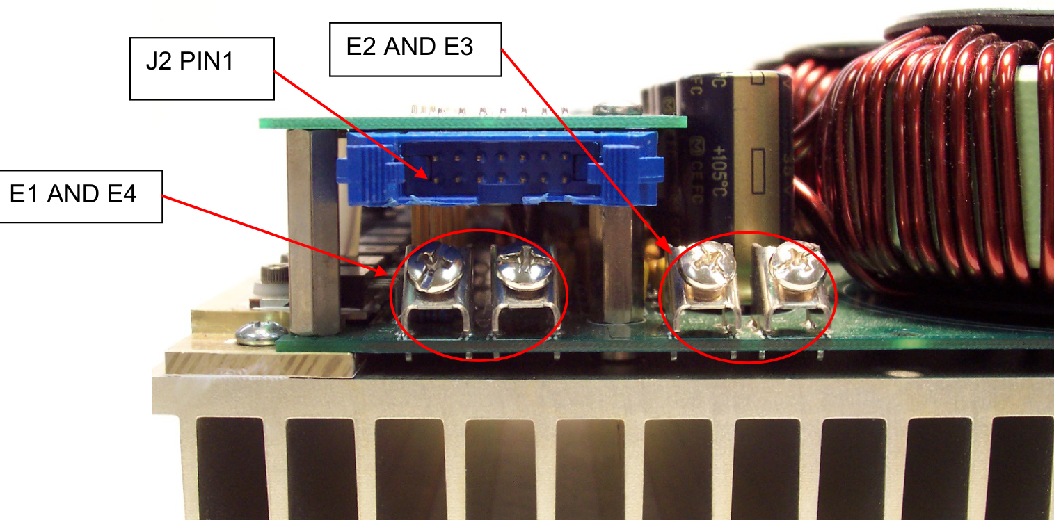
The +24 VDC input are screw terminals located on the main circuit board. Connectors E1 and E4 are +24 VDC. E2 and E3 are ground. These connectors are shown in the photo below:
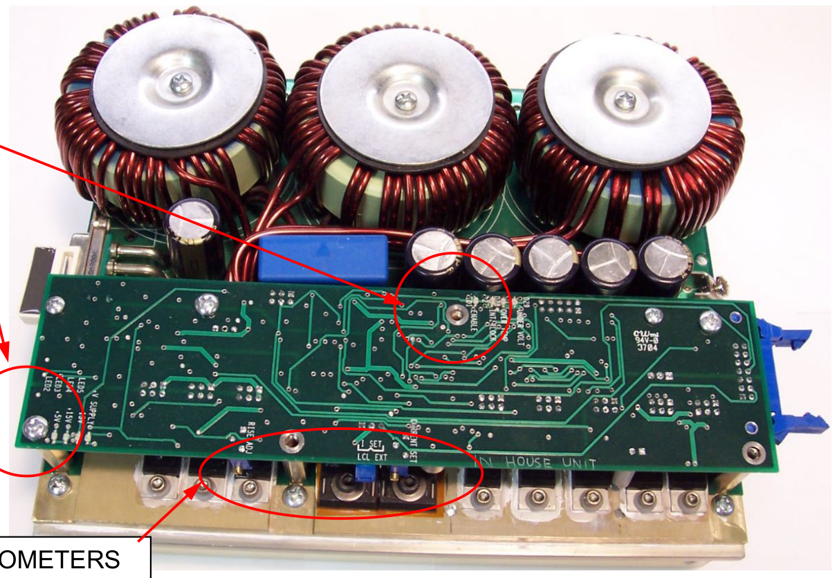
The output current is set by the Current Set potentiometer, located on the edge of the smaller logic circuit board. The current may also be set by a remote analog input. See Section 5 for more details.
The variable rise time is adjusted by the Rise Time potentiometer, located on the edge of the smaller logic circuit board.
All potentiometers can be adjusted while the unit is operating. A suitable insulated adjustment tool should be used. Actual operation is usually necessary so that the correct waveforms can be made and adjusted to suit the user's needs. The photo below shows the location of the control potentiometers, jumpers, and indicator LEDs:
5. Operating Instructions
- Do not remove the input or output cables while the driver is in operation. Do not operate the driver without an appropriate load connected to the output stripline. Failure to observe these precautions can result in potential electric shock to personnel, arcing, and damage to the connectors and system.
- Pulsed-power systems are capable of random triggering via transients. Therefore, when the pulse generator is turned on, or high voltage is present in the chassis, assume it is possible to get a pulse on the output connector.
5.1 Output Stripline
The PCO-6131 is provided with a low-impedance output stripline cable. The laser diode should always be connected to the driver using this stripline cable. Wire or twisted pair are too inductive and may seriously degrade the fidelity of the output current waveform.
5.2 Load Interconnection
The output is provided on a high-current PCB-mount DSUB connector, Amphenol #77TW-C-8W8-S-MP3V-4R or Connector #3008W8SXX57A30X, terminated with a low-inductance stripline cable. Pins 2, 4, 6 & 8 of the connector are the positive pulse output, and pins 1, 3, 5 & 7 are the return.
The output stripline is marked with a + and −. The "+" side is the positive output pulse, and the "−" side of the stripline is the return. The laser diode anodes connect to the "+" side of the stripline, and the laser diode cathode connects to the "−" side. A magnet is mounted to the housing to activate the magnetic reed switch.
The laser diode should be connected directly to the end of the stripline. If wire interconnections are needed between the end of the stripline and the diode, they should be kept as short as possible, preferably no more than 2″ (5 cm) to minimize interconnection inductance. Excessive inductance in the interconnections or laser diode package may lead to ringing on the leading edge of the pulse waveform. This ringing may be reduced or eliminated by lengthening the pulse rise time using the variable rise-time feature.
5.3 Gate Input
An input gate of +5 V ±1 V (CMOS) is required to gate on the PCO-6131. Departure from these values can result in a loss of performance. This trigger requirement is met by any high-quality low-voltage pulse generator.
The gate signal should be connected to J2-8 using a 50 Ω coaxial cable. The shield of the coaxial cable should be connected to any one of the ground pins of connector J2. To improve pulse fidelity, all connections should be as short as possible. The output pulse's width and frequency follow the width and frequency of the input gate. To generate a CW output, the gate should be held high.
5.4 Enable Input
The "enable" signal (J2-10) is used to enable and disable the output of the PCO-6131. This input must be pulled TTL "High" to enable the driver. This input can be connected to an interlock or key switch in the user's system, or may be controlled by the system's control computer.
When the driver is enabled but not pulsing, it dissipates a fixed amount of power (see Section 5.5 below). Therefore, for optimum efficiency and minimum power consumption, the driver should be disabled when not in use.
5.5 Output Current Setpoint Monitor
The output current setpoint monitor (J2 Pin 6) can be used to set the output current flowing in the inductor prior to generating an output pulse. This allows the user to set the current that will be applied to the diode, without applying power to the diode. To set the current using the setpoint monitor, the PCO-6131 must be enabled while the gate input is held low.
5.6 Internal and External Current Setpoint
In internal mode, the potentiometer labeled Current Set controls the output current amplitude. 0 A is full counterclockwise. The output current setpoint monitor may be used to set the output current without applying a pulse to the laser diode.
The external current setpoint (J2 Pin 4) allows the user to apply an external voltage to the potentiometer circuit. The on-board potentiometer then can be used as a range scaling potentiometer. To use this feature, the Current Set External/Local jumper must be set to the External setting (see Figure 2). If the jumper is set to the Local setting, this input is not used.
For example, to use a 0–10 V input and scale the output accordingly, the potentiometer may be adjusted to correlate the maximum output current to 10 V maximum input. In the local mode with the unit enabled and the gate input held low, set the potentiometer to 0 A output, and then change the jumper to External mode. Apply the maximum input voltage desired to the Current Setpoint Input (i.e., 10 V). Then slowly adjust the current setpoint potentiometer until the desired output current is obtained on the Output Setpoint Monitor.
5.7 Leading Edge Risetime Control Potentiometer
The PCO-6131 features a user-adjustable variable rise-time control. This feature allows the user to adjust the rise time within a range of <30 ns to >2.5 µs by means of the PCB-mounted potentiometer (see Figure 2), to optimize the driver's rise time for the user's application. In applications in which the laser diode or interconnection between the driver and the diode is somewhat inductive, the fast rise time of the PCO-6131 may induce ringing on the leading edge of the pulse. The rise time may be slowed down using the variable rise-time control to minimize or eliminate this ringing.
Full counterclockwise is the fastest rise time, and full clockwise is the longest rise time. Please note that this feature does not affect the pulse fall time.
5.8 Indicator LEDs
Several LEDs on the driver logic board may be used for verification of functionality and for troubleshooting. The LEDs and their functions are listed below:
| LED | Function |
|---|---|
| LED1 | Enable Indicator. If the driver is enabled, the LED will be illuminated. If it is disabled, the LED will be off. |
| LED2 | +5 VDC Monitor. If the +5 VDC on-board regulator is functioning correctly, this LED will be illuminated. |
| LED3 | +15 VDC Monitor. If the +15 VDC on-board regulator is functioning correctly, this LED will be illuminated. |
| LED4 | −15 VDC Monitor. If the −15 VDC on-board regulator is functioning correctly, this LED will be illuminated. |
| LED5 | +24 VDC Monitor. Indicates +24 VDC is applied to the driver. |
| D27 | Interlock Fault. Indicates the interlock reed switch is open. |
| D28 | Over-Temperature Fault. Indicates maximum heat-sink temperature has been exceeded. |
| D29 | Under-Voltage Fault. Indicates input voltage is below 18 volts. |
5.9 +24 VDC Input
The +24 VDC input provides the power for the output current. This voltage may be in the range of +20 V to +28 V. It may be unregulated if it does not vary below 20 V or above 28 V.
At 125 A output, the driver dissipates ~75 W when enabled but not pulsing. Efficiency is therefore the ratio of output power to the input power, or η = output power / (idle power + output power). The idle power consumption varies non-linearly with output current and can be approximated by the formula P = I2 × 0.005, where I is the output current. For example, at 75 A output current, the idle power consumption is 752 × 0.005 = 28 W.
The +24 VDC support power should be sized for the average output power (power × duty cycle) plus the idle power consumption as defined above, and an additional 20% for pulse switching losses.
5.10 Power-Up Procedures
The unit should be powered up using the following procedures:
- Before connecting the input pulse generator to the PCO-6131 pulser, set up the pulse generator output to deliver a CMOS-level pulse with a repetition rate and pulse width appropriate for the laser diode being driven. Before connecting input connector J2 to the driver, turn off or disable the output of the pulse generator.
- Connect the input connector J2 prior to applying +24 VDC support power.
- Connect the +24 VDC support power to connectors E1, E2, E3, and E4.
- Connect the laser diode to the output connector using the stripline.
- Apply +24 VDC (±4 V) power to the module.
- To set the output current prior to enabling the output, follow the procedure in steps 7–10 below.
- Ensure that the input gate signal is low (i.e., the input pulse generator is turned off or is disabled).
- Enable the PCO-6131 by pulling the enable input HIGH.
- Monitoring the voltage of the Output Current Setpoint Monitor (J2 Pin 6) with an oscilloscope or digital voltmeter (DVM), set the output voltage to correspond to the appropriate output current by adjusting the Current Set potentiometer. See Section 5.6 for remote current-set instructions.
- When the current is set to the appropriate level, disable the output by pulling the enable input LOW.
- If the output current has not been set using the Output Current Setpoint Monitor and the procedure detailed above, turn the Current Set potentiometer fully counterclockwise (to set the output current to zero).
- Enable the PCO-6131 by pulling the enable input HIGH.
- Turn on or enable the input gate signal.
- If the output current has not been preset, slowly turn up the output current by turning the Current Set potentiometer clockwise. The PCO-6131 should produce an output pulse, with a pulse width and pulse recurrence frequency following that of the incoming gate. The output pulse current may be monitored using the optional PCA-9155. Scaling is 1000 A/V into 50 ohms.
- If there is no output from the PCO-6131, or the output is severely distorted, disable the output and turn OFF the +24 VDC power supply. Leave the PCO-6131 connected to the DC input support power without voltage applied and with all connectors in place for approximately one minute to bleed off the stored energy, then disconnect the DC power to the unit and refer to the Troubleshooting section of this manual.
5.11 Power-Down Procedures
- Disable the output.
- Turn off the +24 VDC power supply.
- Leave the PCO-6131 connected to the +24 VDC input with the voltage turned off and with all connectors in place for approximately one minute to bleed off the stored energy.
- Disconnect the DC support power to the unit.
6. Laser Diode Interconnection Inductance
Application of the PCO-6131 requires attention to detail to prevent problems with inductance in the leads and load. BNC has tested the PCO-6131 with laser diodes to determine how best to apply high-current pulses to laser diodes, and the result of this investigation is presented below.
A stripline is integral to obtaining good fidelity of current pulses. The stripline shown in the figures in this note is the stripline supplied with the PCO-6131 and is available from BNC.
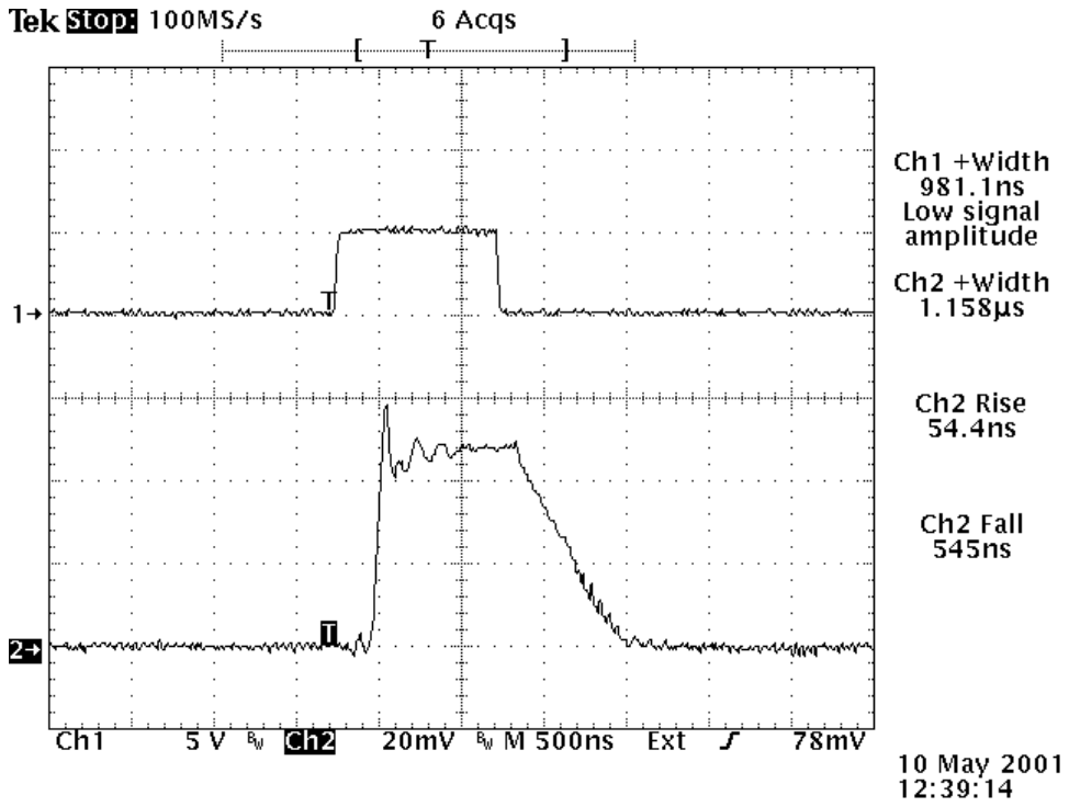
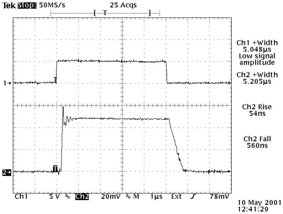
When a stripline is used and connected directly to the laser diode, the fall time was in the range of 500 ns. When the laser diode was connected to the stripline with about 6 inches of wire, the fall time degraded to about 6 microseconds. Inductance negatively affects fall time, and the performance seen with these two interconnection topologies is consistent with the inductance introduced into the circuit by the wire interconnections.
For all tests, the laser diode was driven at approximately 50 amperes. A diode forward voltage of about 2.4 V was measured, confirming that the laser diode was correctly wired into the circuit. The repetition frequency was limited to a few hertz, eliminating the need to heatsink the laser diode.
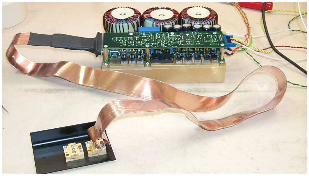
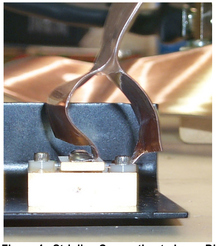
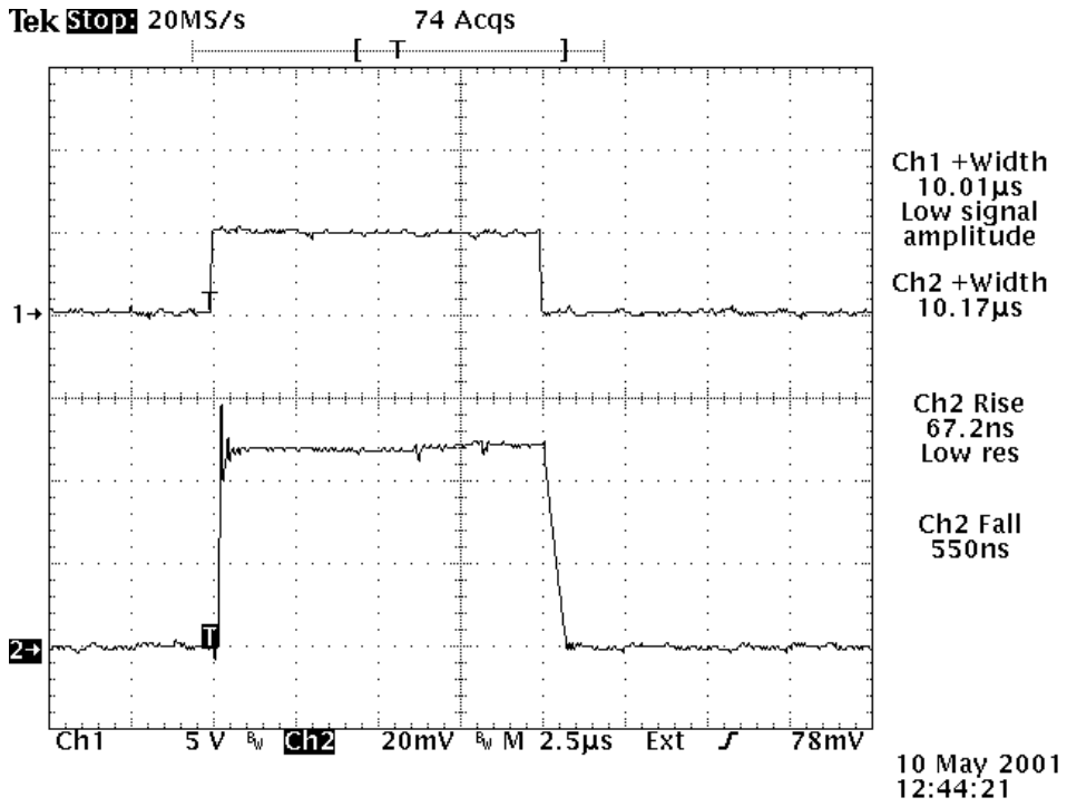
Figures 4 and 5 show how the output stripline was connected to the laser diode for the first set of tests. In Figure 4, the stripline was intentionally separated to show the connections. Normally it is best if the stripline conductors are closely coupled to each other to minimize inductance.
Using this interconnection, at 50 A output the following electrical performance was measured. For all photos, the top trace is the input gate to the PCO-6131, and the bottom trace is the output current pulse measured with the PCO-6131's current monitor.
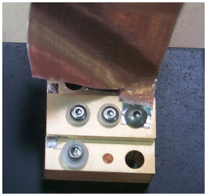
We then connected the laser diode to the PCO-6131 output stripline using approximately 6 inches of wire. Ring lugs were used to attach the wires to the laser diode, and the other ends of the wires were soldered to the ends of the striplines. This interconnection is shown in Figure 9.
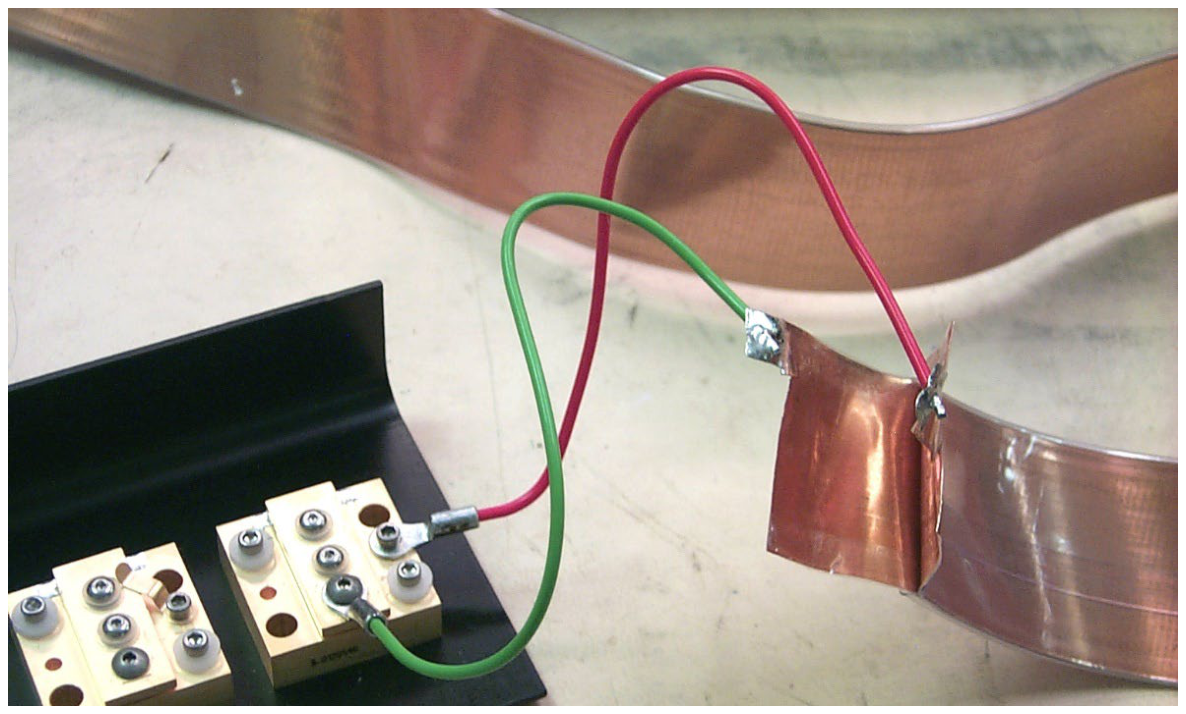
Using this interconnection, at 50 A output the following electrical performance was measured. For all photos, the top trace is the input gate to the PCO-6131, and the bottom trace is the output current pulse measured with the PCO-6131's current monitor.
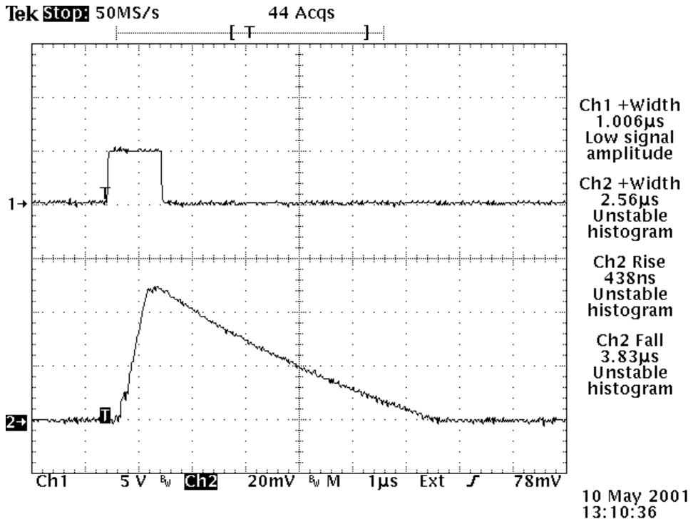
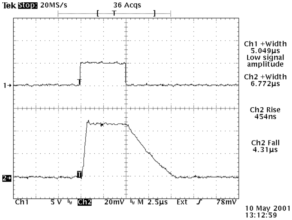
As can be seen from the data above, even the inductance of 6 inches of wire in the connection between the stripline and the laser diode can result in a 5× to 8× degradation in the rise time and fall time.
7. Troubleshooting
7.1 Troubleshooting Procedures
The table below summarizes potential problems and their solutions. If these recommendations do not resolve the problem, BNC customer service can be contacted for further assistance.
| Symptom | Solutions |
|---|---|
| No output pulse | No input gate. Input gate voltage too low. Input gate pulse width too short (increase width). Input gate frequency too high (reduce frequency). No +24 VDC input voltage (check input supply and connections). Enable circuit not satisfied. Output not connected correctly (check all cables and connections). Pulser is damaged (contact BNC customer service). |
7.2 Factory Service
If the procedures above fail to resolve an operational problem, please contact the factory for further assistance:
Berkeley Nucleonics Corporation
2955 Kerner Blvd. #D
San Rafael, CA 94901 USA
Call: (415) 453-9955
Email: info@berkeleynucleonics.com
Web: www.berkeleynucleonics.com/rma-forms
8. Warranty
Berkeley Nucleonics Corporation (BNC) warrants equipment it manufactures to be free from defects in materials and factory workmanship under conditions of normal use, and agrees to repair or replace any standard product that fails to perform as specified within ninety (90) days after the date of shipment to the original owner. PCO-6131 and other OEM, modified, and/or custom products are warranted, as stated above, for ninety (90) days from the date of shipment to the original owner. This warranty shall not apply to any product that has been:
- Repaired, worked on, or altered by persons unauthorized by BNC in such a manner as to injure, in BNC's sole judgment, the performance, stability, or reliability of the product.
- Subjected to misuse, neglect, or accident; or
- Connected, installed, adjusted, or used otherwise than in accordance with instructions furnished by BNC.
BNC reserves the right to make any changes in the design or construction of its products at any time, without incurring any obligation to make any change whatever in units previously delivered.
BNC's sole obligation, and the buyer's sole remedies, under this agreement shall be limited to a refund of the purchase price, or at BNC's sole discretion, to the repair or replacement of products in kind that prove, to BNC's satisfaction, to be defective, when returned to the BNC factory, transportation prepaid by the buyer, within the warranty period. BNC shall in no way be liable for damages consequential or incidental to defects in its products, for failure of delivery in whole or in part, for injuries resulting from its use, or for any other cause.
Returns must be preauthorized and accompanied by a BNC return RMA number. Return Material Authorization can be initiated from the Berkeley Nucleonics website at https://www.berkeleynucleonics.com/rma-form.
The foregoing states the entire warranty extended by BNC and is given and accepted in lieu of (1) any and all other warranties, expressed or implied, including but not limited to the implied warranties of merchantability and fitness for any particular purpose, and (2) any obligation, liability, right, claim, or remedy in contract or tort.