Introduction
This document describes how to use the BNC Series Serial Data Pattern Generator to generate the signals for the testing and characterization of standard logic gates, as well as all generic digital systems. The BNC Series Serial Data Pattern Generator simplifies the multilevel pulse generation thanks to its features that combine the pulse and edge shaping with the ability to reproduce a multilevel programmed pattern. Considering the amplitude of 12 Vpp into 50 Ohm (24 Vpp into open) joined to an analog shift of ±6 V into 50 Ohm (±12 V into open) and the maximum symbol rate of 300 Mega-Symbols per second, this instrument finds application as a replacement of the Agilent 81110A series.
| Key Issues | Characterize digital logic gates and integrated circuits. |
|---|---|
| Solutions | Model 675 & 685 Serial Pattern Generators; Teledyne, LeCroy, WaveRunner 620Zi. |
| Results | Accelerate research, reliability, and failure analysis studies of semiconductor devices. Reduce the time from setup to running characterization of digital logic gates. |
Model 675 & 685 SPG Key Features
Up to 4 logic levels
Each channel can define up to 4 independent voltage levels and emulate, in addition to logical ‘0’ and ‘1’, a tristate buffer or a weak ‘0’ signal when a bus is not driven.
Edge Definition
The shape of each transition between the levels can be arbitrarily defined by the user. This feature is capable of shaping the edge as RC transient, or to add a positive overshoot. The 14-bit DAC resolution along with the 318 MHz analog bandwidth provides you an excellent signal fidelity.
Amplitude
The BNC Serial Data Pattern Generators can reach up to 12 Vpp amplitude at 50 Ohm (24 Vpp into open); furthermore, a programmable hardware offset (called baseline offset) is available which allows shifting the voltage window of ±6 V at 50 Ohm (±12 V into open). By using the baseline offset, the instrument can generate a 0 - 12 V signal at 50 Ohm (0 - 24 V into open).
Multi-Instrument synchronization up to 32 channels
Each unit has 8 independent analog channels which can be synchronized with up to 4 units to build a 32-channels system.
Fine time resolution
Thanks to DDS technology, the skew between the channels can be controlled with a resolution on the order of 1 ps.
Generation
- Continuous: the generation starts when the user presses the Start button and it ends when the user presses the stop button.
- Burst: the instrument waits for a trigger and then the pattern is generated for the selected number of times. At the end of the burst the instrument waits for a new trigger.
- Modulation: the instrument applies an AM, FM, PM, FSK or PSK modulation to the generated pattern.
Selectable Header
The memory depth allows a pattern length up to 2 Mbits, but it is possible to select an initial part of the total pattern that is generated once while the rest of the pattern is repeated more times.
Intuitive User Interface
The user interface allows you to easily program the instrument, using the touch screen and the physical keyboard. If you need to integrate the instrument into an automatic testbench, the AT-AWG-4010 Series Data Pattern Generator can be controlled by an external controller via SCPI command.
Standard Logic
Standard logic gates are the basic logic blocks which compose all digital circuits. The development of digital applications is realized through programmable IC such as MCU (MicroController Unit) or PGA (Programmable Gate Array), the discrete gates still find applications when the designers need a function that can’t be realized directly in the programmable IC or if the application is not complex enough to include a programmable IC on the board.
In some cases, it is necessary to add external logic gates to reach a bit rate that a programmable device cannot support, or to insert a level shifter allowing the communication between IC with different voltage standards or to insert a multiplexer in order to increase the number of pins of an MCU.
There are many types of devices from different logic families (TTL, CMOS, BiCMOS, etc.) with the same logical function. To characterize and test them, from the simplest ones such as the single gates (NOT, NAND, NOR, and so on) to the more complex types, such as multichannel latches and counters, it is necessary to generate signals with specific characteristics in term of edge shaping, overshoot, amplitude, etc. It is necessary to remember that the digital signals are not ideal, however in real-world applications, they take a bit of time to switch and can be affected by overshoot, so the best test signal is an analog signal which allows the user to test a specific feature.
For all the previously described applications, the BNC Series Serial Data Pattern Generator is the ideal solution, due to its ability to combine the digital pattern with the analog characteristics like edge shaping, amplitude, noise and, modulation of the analog front end.
The following section will illustrate how to generate the signals needed for the digital tests using the Serial Data Pattern Generator, with an example report on a typical application.
A. Measurement of the Propagation Delay of Asynchronous Logic Gate
The following application considers a 3 input AND gate, but the principle remains valid for every logic network. It is known that the 3 inputs of the AND gate are logically equivalent, but the analog characteristics such as the propagation delay depends on the internal architecture.
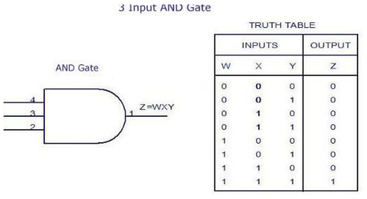
Using the BNC Series Serial Data Pattern Generator, the user can define analog characteristics of the signals on each input of the gate under test, setting the voltage level and the edge shaping independently among the channels.
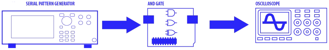
The figure below shows the connections for this test:
- The 1st, 2nd and 3rd channels of the pattern generator are connected to the input of the AND gate.
- The 4th channel is connected to oscilloscope as reference.
- The Output of the AND gate is connected to the oscilloscope.
- For simplicity: the power supply, ground and other components needed for the proper operation of the AND gate has been omitted.
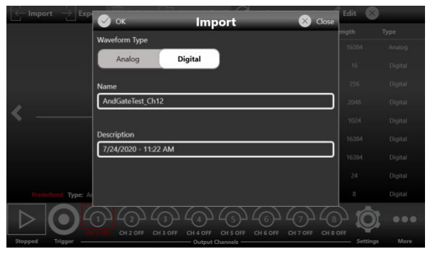
How to configure the Pattern Generator using the software interface
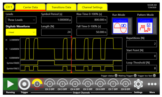
1. From the “Carrier Data” tab, set the level number to 2, define the bit rate and select Custom as Pattern Mode.
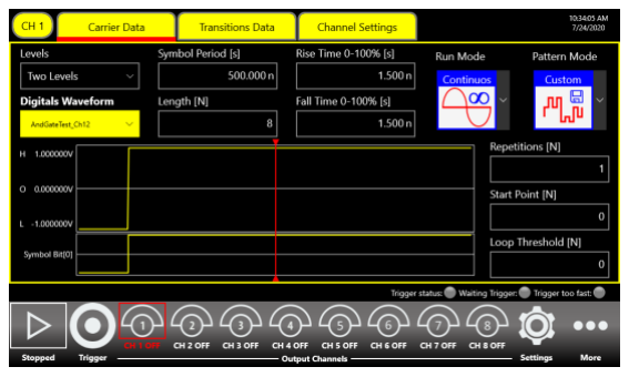
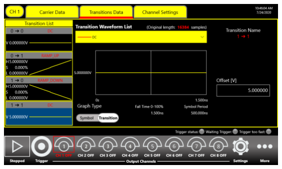
2. From the “Transition Data” tab, define the shape of the edges; for this example, the value was set as linear, defining a rise/fall time of about 4 ns. Define the levels by setting the voltage levels of each transition.
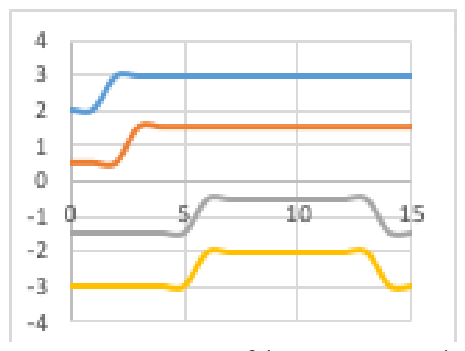
4. Definition of the pattern:
| Ch 1 | 01111111 |
|---|---|
| Ch 2 | 01111111 |
| Ch 3 | 00011110 |
| Ch 4 | 00011110 |
| Ch 5 – 8 | not used |
In order to evaluate the propagation delay of input 3, inputs 1 and 2 go to high level at the same time, once they are stable, input 3 executes the rising edge, stays at high level for 4 symbols and then executes a falling edge. The channel 4 behaviour is the same of the channel 3 and is used as reference for the oscilloscope.
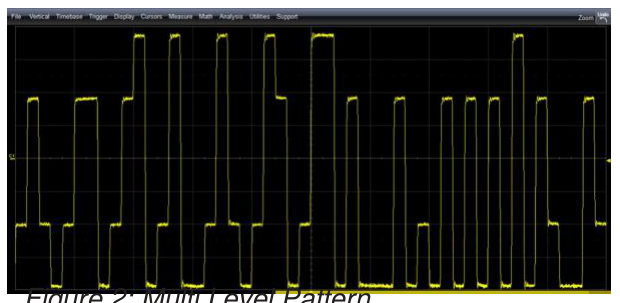
5. Press the Run button and observe the results.
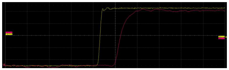
The delay between the output of the logic gate and the channel 4 of the SPG is presented in the oscilloscope screenshot above.
Note: to compensate for the delay of the cables the user can adjust the initial delay of channel 4. This setup is useful in characterizing the input-to-output propagation delay for input 3, but by changing the pattern the user can also observe the behavior of other inputs.
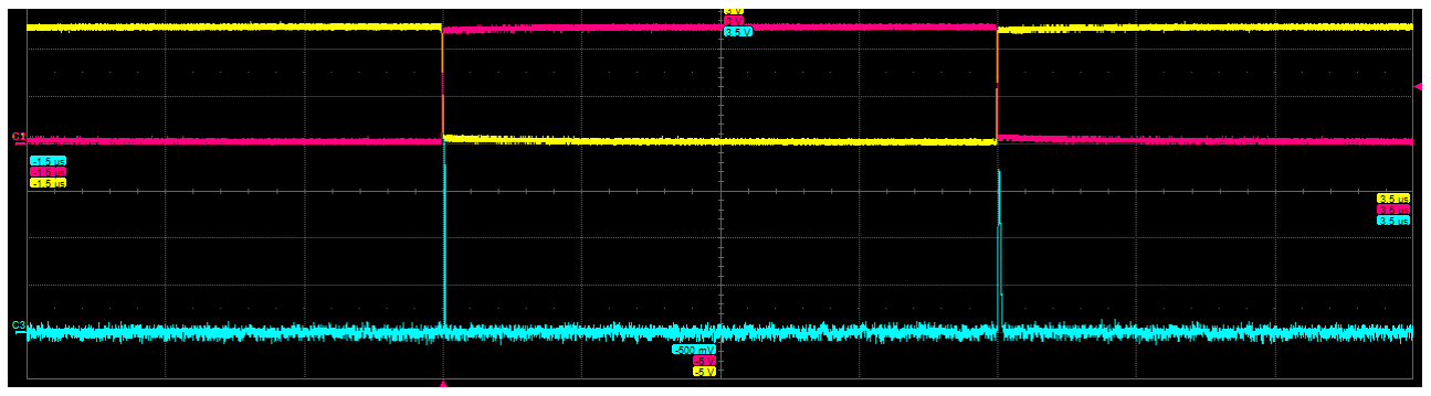
B. Effects of Simultaneous Switches in Asynchronous Logic
When working with asynchronous logics, it can be interesting to investigate the behavior of the logic gate at the simultaneous switch of two or more inputs. So starting from the previous set-up, for this example, the goal was to test what happens if the 1st input run at high level while the 2nd input run at low level.
The following pattern was loaded:
| Ch 1 | 11000011 |
|---|---|
| Ch 2 | 00111100 |
| Ch 3 | 11111111 |
| Ch 4 – 8 | not used |
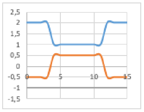
Logically the output should be always ‘0’, but depending on the edges of the input signal and on the internal architecture of the logic gate under test, it is possible to see a spike on the output. The pictures below show that, although the output should be always 0, there are 2 spikes at the input switches.
To summarize, below are oscilloscope screenshots from other tests, obtained by varying the rise/fall time and the skew between the channels.
- Skew channel 1 – 2: 2 ns
- Rise / Fall time: 4 ns
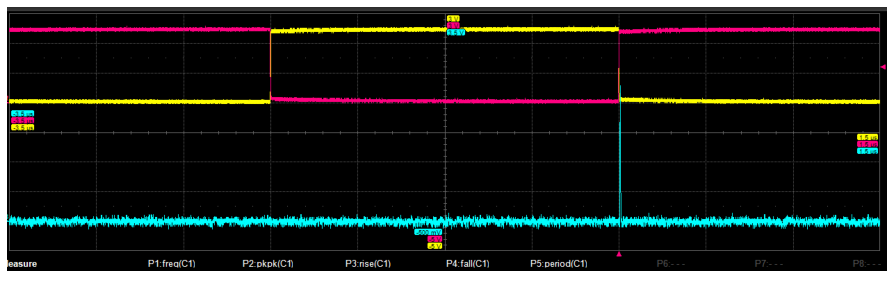
As is apparent in the picture above, adding a skew on the output generates a spike when the 1st input switches to high level.
- Skew channel 1 – 2: 0
- Ch 1 Rise time 7 ns
- Ch 1 Fall time 4 ns
- Ch 2 Rise time 7 ns
- Ch 2 Fall time 4 ns
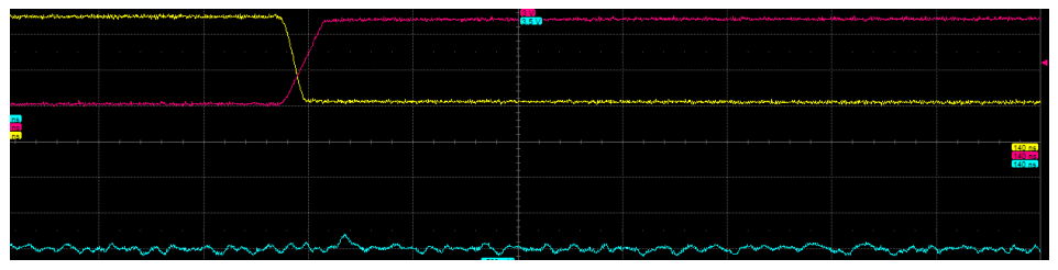
Applying the setting above results in no spike being recorded.
Conclusion
The Model 675 & 685 Data Pattern Generators offers a set of tools to address the most complex applications in digital devices characterization. Multiple outputs, high voltage window, custom and modulated pattern generation are unique features which can help designers test their devices with confidence; the ease to use user interface allows the user to simplify and speed up the setup of the most complex systems.
About Us
Berkeley Nucleonics Corporation (BNC) is a leading manufacturer of precision electronic instrumentation for test, measurement, and nuclear research. Our corporate headquarters are in San Rafael, California, with additional manufacturing facilities and sales offices located throughout the United States.
Contact Information
Berkeley Nucleonics
2955 Kerner Boulevard
San Rafael, CA 94901
- General Information: info@berkeleynucleonics.com
- Sales Department: sales@berkeleynucleonics.com
- Technical Support: support@berkeleynucleonics.com
YouTube Channel: please subscribe to our channel to stay up to date on the latest product videos and tutorials.