Why the Clock Source Matters
In new digital designs and high-speed data converters, the quality of the clock source is crucial. These systems depend heavily on a clock source that offers minimal jitter to maintain signal integrity.
The Model 865B stands out in this context, offering exceptionally clean clock signals. The performance of digital designs and data converters is directly influenced by the quality of their clock source. To maximize the efficiency of a data converter, an optimal clock source is essential. This is particularly important for maintaining the signal purity in digital-to-analog converter (DAC) outputs and in capturing the data accurately in analog-to-digital (ADC) converters.
As clock rates continue to rise, the demand for high-quality signal integrity becomes even more stringent. Therefore, a versatile and reliable clock source that can deliver the necessary signals with minimal jitter, low noise, and superior spectral purity is indispensable for current and future digital design needs.
The Model 865B is renowned for generating the cleanest signals, making it an ideal clock source. It boasts an RF output frequency that reaches up to 20 GHz, catering to the advanced and future generation DACs and ADCs that require increasingly higher clock rates.
Key Specifications
| Frequency Range | From 100 kHz to 12.75 / 20 / 26 / 40 GHz |
|---|---|
| Superior SSB Phase Noise | -130 dBc (1 Hz) at 1 GHz with a 1 kHz offset |
| Exceptionally Low Jitter | 1 ns at 1 GHz over a 1 Hz to 10 MHz bandwidth |
| Negligible Wideband Noise | -150 dBc at 1 GHz with a 10 MHz offset |
Minimizing Wideband Noise
The Model 865B's ability to minimize wideband noise is particularly vital for clock source applications. In scenarios like ADC testing, the clock signal's wideband noise can accumulate, leading to a reduction in the overall signal-to-noise ratio, necessitating careful consideration.
A versatile clock source must deliver optimal RF performance across the entire frequency spectrum, as high-speed devices are also tested and specified at lower frequencies. The Model 865B employs a direct concept down to 8 kHz, ensuring top-notch RF performance across its full range.
Harmonic and Subharmonic Suppression
In the past, filters were needed to mitigate harmonics and subharmonics. However, the Model 865B's built-in harmonic filter and excellent subharmonic suppression capabilities make such filters redundant. Its features include:
| Harmonic Suppression | 60 dB from 100 kHz to 12 GHz |
|---|---|
| Broad Frequency Range Harmonic Suppression | 50 dB from 100 kHz to 12 GHz |
| Nonharmonics | Below -92 dBc (typical) at 1 GHz for a range of 1.25 Hz to 2.5 GHz |
| SSB Phase Noise | -130 dBc (1 Hz) at 1 GHz with a 1 kHz offset |
| Ultra-Low Wideband Noise | -150 dBc at 1 GHz with a 10 MHz offset |
Overcoming Cable Losses
In some testing scenarios, extensive cabling is required, which can lead to significant signal attenuation. This issue becomes increasingly critical at higher clock frequencies. The Model 865B is designed to counteract these losses effectively, eliminating the need for external amplifiers:
| For the 40 GHz Model | Delivers up to 15 dBm from 8 kHz to 100 kHz (Option 8K), up to 25 dBm within a 6 GHz range, and up to 18 dBm from 26 GHz to 40 GHz. |
|---|---|
| For the 20 GHz Model | Provides up to 26 dBm in the 5 GHz frequency range and up to 20 dBm in the 20 GHz range. |
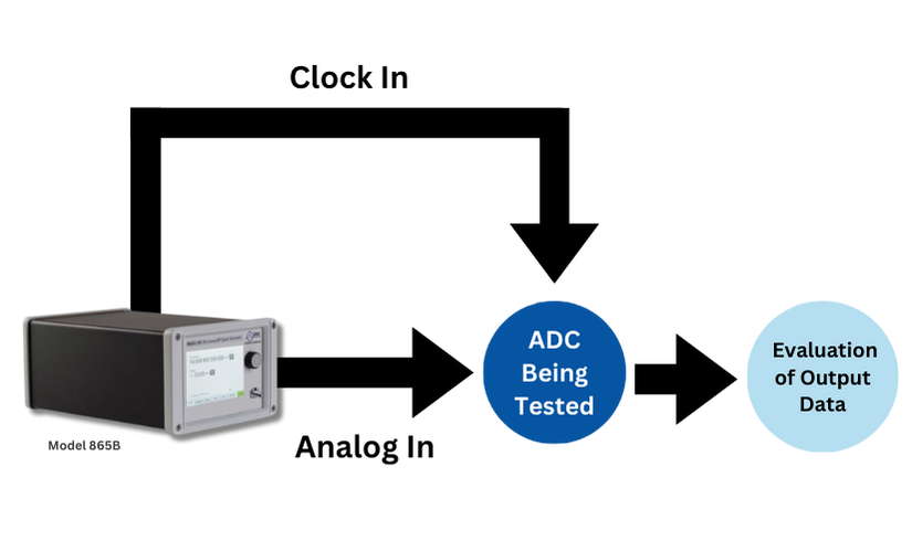
The Model 865B features a unique electronic attenuator, ensuring high level control without any wear and tear. This makes it ideal for compact ADC testing setups, requiring only a single Model 865B even if an integrated second source is needed.
The Optional Second Source
The optional second source within the Model 865B, offering exceptional purity up to 6 GHz, is a notable advantage. Its specifications include:
| SSB Phase Noise | -130 dBc (1 Hz) at 1 GHz with a 1 kHz offset |
|---|---|
| Ultra-Low Wideband Noise | -150 dBc at 1 GHz with a 10 MHz offset |
The Model 865B boasts a feature where its frequency and level settings are completely independent of the RF output. This is particularly beneficial in ADC testing, as a single instrument can simultaneously provide both the RF input and the clock signal. The output of the Model 865B can be configured either as a standard sine wave or a square wave. To facilitate a direct connection to the Device Under Test (DUT), it supports both single and differential output formats, including the option to apply a DC offset. The second source is notably versatile, offering adjustable levels and frequencies.
Straightforward Upgrade and Integration
Upgrading to the Model 865B from an existing clock source solution is straightforward. It is designed to support remote programming emulation compatible with many common platforms from various vendors. With its compact 2 HU form factor, the Model 865B is designed to easily integrate into any available space in your setup. Please check out the product page for additional information: https://www.berkeleynucleonics.com/model-865